

 Product
 Brand
Brand Articles
 Tools
Tools
What is the Difference between an Integrated Circuit and a Chip

What Is An Integrated Circuit (IC)
The shortest accurate answer is therefore: IC describes the integrated electronic circuit; chip is an informal name whose physical meaning depends on context. Packaging is not what turns a non-chip into a chip under every accepted usage.
1. IC, chip, die, and package are related, not opposing terms
NIST defines an integrated circuit as many transistors combined into a small circuit on a chip. Its public semiconductor glossary uses chip for a self-contained semiconductor piece packaged for use in electronics. Intel gives the useful industry caveat: the definition of chip is less rigid, and the word can refer to a single die even though the public usually encounters the packaged version.
That variation is why the original question cannot be answered with a strict equation such as "IC = internal silicon" and "chip = black package." The more dependable vocabulary is below.
| Term | Precise working meaning | What it is not |
|---|---|---|
| Semiconductor | A material whose electrical behavior can be controlled; silicon is the dominant base for many ICs | Not automatically an IC |
| Wafer | A circular semiconductor slice on which many copies of an IC are fabricated | Not one finished component |
| Integrated circuit (IC) | A circuit with active and passive elements formed and interconnected as an integrated structure | Not the protective package by itself |
| Die | One rectangular piece separated from a processed wafer; it carries one IC design or a repeated instance of it | Not necessarily ready for normal PCB assembly |
| Chip | Informal, context-dependent term for a die, an IC, or a packaged semiconductor product | Not a reliable manufacturing-stage label |
| Package | The structure that supports and protects one or more dies and provides electrical and thermal connections | Not the IC circuitry itself |
| Packaged IC | The sellable component that combines an IC die with package interconnects and external terminals | Not always a single-die device |
| Chiplet | A die-level functional building block intended to be integrated with other dies in one package | Not simply any small packaged IC |
| System in Package (SiP) | Multiple dies and, in some implementations, other components integrated in one package | Not the same as a single-die system-on-chip |
When can IC and chip be used interchangeably?
In general technology writing, "memory chip," "processor chip," and "integrated circuit" may point to the same commercial product. Texas Instruments itself describes chips as integrated circuits in public-facing material. That usage is normal.
Precision matters when the physical form affects the work. A procurement record needs the complete ordering code and package. A failure-analysis report should distinguish a cracked die from a damaged mold compound. A packaging engineer needs to know whether a test occurs at wafer, singulated-die, package, or system level.
2. From wafer to packaged IC
Fabrication creates repeated IC patterns across a wafer. Back-end assembly then tests, separates, connects, protects, marks, and retests those devices. The exact sequence varies by package technology, but the manufacturing boundary is clearer than the word chip.
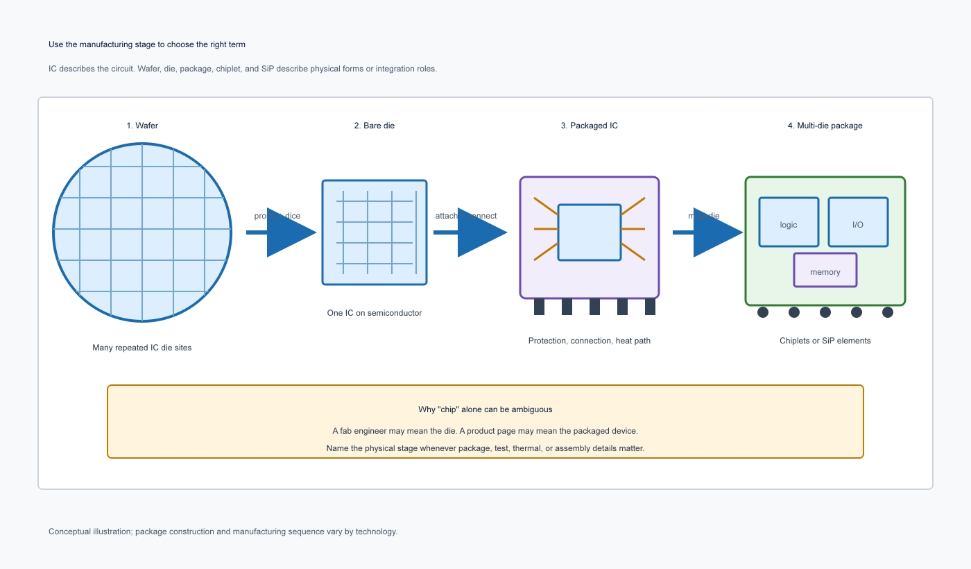
Step 1: fabricate integrated circuits on the wafer
Front-end fabrication forms transistors, capacitors, resistive structures, and interconnect layers on a semiconductor wafer. Lithography is one part of a much larger sequence that also includes deposition, etch, implantation, cleaning, planarization, and inspection. Not every IC uses extreme ultraviolet lithography, and a process-node name does not describe one literal physical dimension across the finished device.
Multiple instances of the same IC design are normally patterned on the wafer. At this stage, engineers may casually call each patterned area a chip, but die site or die is clearer when discussing manufacturing.
Step 2: probe the wafer and separate the dies
Wafer probing electrically tests individual die sites before assembly so that known failures can be screened out. The wafer is then mounted and cut along saw streets. Each separated piece is a singulated die.
Bare die can be sold and assembled directly into a module or hybrid circuit. TI distinguishes its die and wafer products from standard packaged versions, which is direct evidence that a die and a packaged component are different product forms even when they implement the same IC function.
Step 3: attach and electrically connect the die
The die is mounted to a leadframe or package substrate. Wire bonding connects die pads to package conductors one wire at a time; flip-chip assembly instead uses bumps or copper pillars between the die and substrate. The interconnect method affects electrical parasitics, I/O density, thermal paths, package height, and assembly cost.
Step 4: protect, finish, and test the device
Many packages use molding compound or another enclosure to protect the die and interconnects. External leads, lands, pins, or solder balls create the board-level interface. Marking identifies the product, and final testing verifies the packaged device before shipment.
Packaging does more than make a black shell. It provides mechanical support, environmental protection, a heat-flow path, power and signal distribution, and terminals that can be assembled to a PCB.
3. The practical difference between an IC and a packaged device
An IC design can be offered in several physical forms. The circuitry may be substantially the same while the package changes how the product is assembled and used.
| Design question | IC or die consideration | Package consideration |
|---|---|---|
| Function | Logic, memory, analog, RF, power, sensing, or mixed-signal behavior | Does not create the core circuit function, but can integrate additional dies or passives |
| Electrical performance | Transistor architecture, interconnect, voltage, frequency, leakage | Lead and interconnect resistance, inductance, capacitance, signal and power integrity |
| Thermal behavior | Junction power and temperature limits | Junction-to-case/board path, exposed pad, lid, heat spreader, airflow interface |
| Board assembly | Bare die requires specialized attach and interconnect | Leads, lands, pins, or balls determine PCB footprint and solder process |
| Test and reliability | Wafer sort and known-good-die strategy | Package stress, moisture sensitivity, board-level reliability, final test |
| Ordering | Die or wafer sales may use separate suffixes and conditions | Complete part number normally identifies package and shipping form |
The package can materially change usable performance. A low-inductance package can support faster edges or higher current. A thermally limited package can prevent a die from operating at the power it could otherwise deliver. Two ordering codes with the same base IC name therefore should not be treated as interchangeable until pinout, footprint, thermal data, electrical limits, and qualification are compared.
4. Common IC package families
Package names describe the external connection pattern and construction, not a different definition of integrated circuit. TI's current packaging terminology includes families such as DIP, QFN, BGA, and WCSP.
| Package family | Board connection | Typical engineering reason to choose it | Main design caution |
|---|---|---|---|
| DIP | Through-hole leads in two rows | Easy handling, sockets, education, and legacy equipment | Large board area and limited I/O density |
| SOIC / QFP | Gull-wing surface-mount leads | Visible solder joints and broad assembly support | Lead pitch, board area, and lead inductance |
| QFN / DFN | Flat perimeter contacts, often with an exposed pad | Compact footprint and useful electrical/thermal path | Land pattern, voiding, inspection, and exposed-pad soldering |
| BGA | Array of solder balls beneath the package | High I/O density and short interconnects | PCB escape routing, inspection, rework, and warpage |
| WCSP / DSBGA | Wafer-level terminals with package size close to die size | Very small footprint and low package parasitics | Board flex, handling, underfill strategy, and fine-pitch assembly |
Package selection is a system decision. Pin count alone is not enough; PCB capability, thermal target, mechanical loading, inspection method, lifecycle, cost, and manufacturing yield all matter.
5. How chiplets and advanced packaging change the picture
Traditional explanations often assume one die per package. That model still exists, but it no longer describes every high-performance or highly integrated product.
Advanced packaging can place multiple dies side by side, connect them through a bridge or interposer, or stack them vertically. Intel describes companion dies connected with advanced packaging as chiplets and uses 2.5D and 3D technologies to connect logic and high-bandwidth memory. UCIe standardizes a package-level die-to-die interface to support interoperable chiplet systems.
Chiplet versus IC
A chiplet usually contains an integrated circuit function, but the word emphasizes its role as one building block in a larger package. One chiplet may provide processor cores, another I/O, another cache, and another analog or accelerator functions. The final package behaves as one product even though it contains multiple dies.
SoC versus SiP
A system-on-chip (SoC) integrates many system functions on one primary die.
A system-in-package (SiP) combines multiple dies, and sometimes passive or other components, within one package.
The boundary can blur in hybrid products: an SoC die may share a package with memory, power-management dies, or radio components. For teardown, sourcing, thermal analysis, and export classification, describe the actual die and package architecture instead of relying on the marketing word chip.
What a process-node name does and does not tell you
Modern node names are technology labels rather than a guarantee that every transistor feature measures the stated number. They also describe die fabrication, not the package pitch or external product size. A product made with an advanced node can still use a much larger package because power delivery, memory, I/O, mechanical support, and cooling require area.
6. Which term should you use?
| Situation | Best term | Example |
|---|---|---|
| General explanation | Chip or IC, with context | "The controller chip contains an integrated circuit." |
| Schematic and component selection | IC, device, or full part number | "Use the IC in the QFN ordering option." |
| Wafer fabrication and yield | Die, die site, or wafer | "Wafer sort identified failing die sites." |
| Packaging and failure analysis | Die, substrate, interconnect, package | "The die is intact, but two bond wires lifted." |
| Multi-die design | Chiplet, die, package, SiP | "The package combines logic chiplets and memory stacks." |
| Purchasing | Manufacturer plus complete ordering code | "The package suffix and temperature grade must match." |
When unsure, ask one clarifying question: Do you mean the circuit design, the bare semiconductor die, or the packaged component? That question resolves most IC-versus-chip confusion immediately.
7. A brief history of the integrated circuit
Jack Kilby demonstrated a working integrated circuit at Texas Instruments in 1958. Robert Noyce subsequently developed a practical monolithic silicon IC concept using planar processing and deposited metal interconnections. The two contributions addressed different parts of the problem and are commonly recognized together in the history of the IC.
The lasting innovation was not a particular black package. It was the ability to form and interconnect circuit elements together on semiconductor material, then manufacture many copies through wafer processing. Packaging made those circuits practical to power, cool, protect, test, and connect to larger systems.
8. FAQ
Is a chip the same thing as an integrated circuit?
Often in ordinary conversation, yes. Technically, integrated circuit describes the electronic circuit, while chip is a flexible term that may refer to the die, the IC, or the packaged product. Use more specific vocabulary when the physical form matters.
Is a die the same as a chip?
Chip is often used for a die in fabrication discussions, but die is the precise term for one piece separated from a semiconductor wafer. The same die may later be assembled into different package options.
Is the package part of the integrated circuit?
The package is physically part of the finished semiconductor device, but it is distinct from the integrated circuitry formed on the die. It protects, supports, cools, and connects one or more dies.
What is the difference between a chiplet and an IC?
A chiplet normally contains an IC function, but it is designed or used as one die-level building block in a multi-die package. The term describes its integration role, not a separate category of electronic circuit.
What is the difference between SoC and SiP?
A system-on-chip integrates many system functions on one primary die. A system-in-package combines multiple dies and potentially other components inside one package. A product can contain an SoC die as part of a larger SiP.
9. References
Texas Instruments, Semiconductor Packaging Assembly Technology.
Computer History Museum, Practical Monolithic Integrated Circuit Concept Patented.
Related Utmel resources
 UTMEL
UTMEL
We are the professional distributor of electronic components, providing a large variety of products to save you a lot of time, effort, and cost with our efficient self-customized service. careful order preparation fast delivery service
1. What does the chip do?
The role of the chip: It can control everything from computers to mobile phones to digital microwave ovens. Although the cost of designing and developing a complex integrated circuit is very high, the cost per integrated circuit is minimized when distributed over products, often in the millions. The performance of integrated circuits is high because the small size brings short paths, enabling low-power logic circuits to be applied at fast switching speeds.
2. Are chips the same as integrated circuits?
Different.
Chip is a general term for semiconductor component products. It is the carrier of integrated circuits, which is divided into wafers.
Chip is an abbreviation of integrated circuit. In fact, the real meaning of the word chip refers to a little large semiconductor chip inside the integrated circuit package, that is, the die. Strictly speaking, chips and integrated circuits are not interchangeable.
Integrated circuits are manufactured through semiconductor technology, thin-film technology and thick-film technology. Any circuit that miniaturizes a certain function and is made in a certain packaged circuit form can be called an integrated circuit.
3. What does a chip have to do with an integrated circuit?
The previous circuits of the chip were all circuits that were connected together by discrete components. After the transistor was invented, the integrated circuit was invented in 1961. This is a revolution in circuit design. It connects the various elements of the entire transistor circuit, and makes it on a semiconductor substrate at the same time, forming an inseparable whole, breaking the concept of the original circuit, breaking the original design method of discrete components, and realizing the The "brain" of a computer and all electronic devices, which is a combination of materials, components, and circuits, is called a microprocessor, or chip.
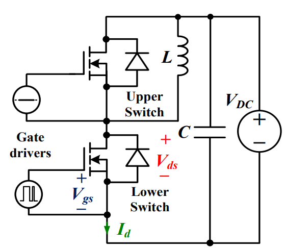 Discovering New and Advanced Methodology for Determining the Dynamic Characterization of Wide Bandgap DevicesSaumitra Jagdale15 March 20242876
For a long era, silicon has stood out as the primary material for fabricating electronic devices due to its affordability, moderate efficiency, and performance capabilities. Despite its widespread use, silicon faces several limitations that render it unsuitable for applications involving high power and elevated temperatures. As technological advancements continue and the industry demands enhanced efficiency from devices, these limitations become increasingly vivid. In the quest for electronic devices that are more potent, efficient, and compact, wide bandgap materials are emerging as a dominant player. Their superiority over silicon in crucial aspects such as efficiency, higher junction temperatures, power density, thinner drift regions, and faster switching speeds positions them as the preferred materials for the future of power electronics.
Read More Applications of FPGAs in Artificial Intelligence: A Comprehensive GuideUTMEL29 August 20255578
This comprehensive guide explores FPGAs as powerful AI accelerators that offer distinct advantages over traditional GPUs and CPUs. FPGAs provide reconfigurable hardware that can be customized for specific AI workloads, delivering superior energy efficiency, ultra-low latency, and deterministic performance—particularly valuable for edge AI applications. While GPUs excel at parallel processing for training, FPGAs shine in inference tasks through their adaptability and power optimization. The document covers practical implementation challenges, including development complexity and resource constraints, while highlighting solutions like High-Level Synthesis tools and vendor-specific AI development suites from Intel and AMD/Xilinx. Real-world applications span telecommunications, healthcare, autonomous vehicles, and financial services, demonstrating FPGAs' versatility in mission-critical systems requiring real-time processing and minimal power consumption.
Read More The 2026 Engineer’s Guide: Choosing the Right MCU for Your Next IoT & New Energy ProjectUTMEL30 April 20261860
A comprehensive comparison of 2026's leading MCUs from ST, NXP, and Microchip across power efficiency, processing performance, connectivity, and ecosystems to help engineers select the optimal chip for next-gen IoT and new energy projects.
Read More AI Server Components: Engineering Next-Gen Data Center Hardware for 100kW RacksUTMEL15 May 20261003
The transition from traditional enterprise IT to AI-driven workloads has rendered legacy data center hardware obsolete, forcing infrastructure planners to re-engineer server components for extreme thermal environments.
Read More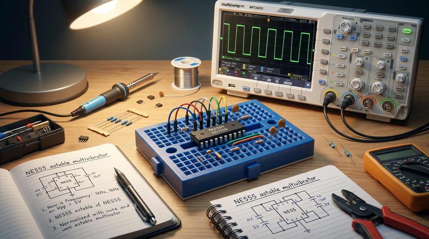 The Practical Engineer’s Guide to the NE555N Timer: Pinout, Setup, and TroubleshootingUTMEL29 May 2026797
This comprehensive guide explores the NE555N timer, detailing its 8-pin layout, internal architecture, and key datasheet specifications. It compares the bipolar IC to CMOS variants and details setup configurations for astable, monostable, and bistable modes. Additionally, the guide offers practical troubleshooting advice to prevent common breadboard failures, such as floating reset pins and electrical noise issues.
Read More
Subscribe to Utmel !
![AD5520JSTZ]() AD5520JSTZ
AD5520JSTZAnalog Devices Inc.
![FOD3184SDV]() FOD3184SDV
FOD3184SDVON Semiconductor
![AT88SC0808CA-SH]() AT88SC0808CA-SH
AT88SC0808CA-SHMicrochip Technology
![AT88SC0204CA-SU]() AT88SC0204CA-SU
AT88SC0204CA-SUMicrochip Technology
![HCS200/SN]() HCS200/SN
HCS200/SNMicrochip Technology
![ACPL-332J-500E]() ACPL-332J-500E
ACPL-332J-500EBroadcom Limited
![FOD8320R2]() FOD8320R2
FOD8320R2ON Semiconductor
![ATECC108A-SSHCZ-B]() ATECC108A-SSHCZ-B
ATECC108A-SSHCZ-BMicrochip Technology
![HCS512-I/P]() HCS512-I/P
HCS512-I/PMicrochip Technology
![PAM8904JER]() PAM8904JER
PAM8904JERDiodes Incorporated


